

VIEW Micro Metrology articles
Wire bonding remains one of the most widely used semiconductor interconnect technologies, supporting applications ranging from power electronics and automotive devices to memory packages and legacy logic. Shrinking wire diameters, combined with material variability across aluminum and copper to gold and palladium coated alloys, have increased inspection complexity, particularly for measuring wire loop geometry, electrical continuity, and bond placement on highly-reflective surfaces. Conventio
If we look around at today’s electronics things are getting smaller day by day but power and performance are only going up. Phones laptops cars even small IoT devices all need to do more work in less space. That is where packaging starts to matter a lot. QFN packaging came in as a practical solution when this shift started happening. It helped engineers manage space without losing performance.
We often see how this type of packaging su
When you look at a modern chip you only see part of what is really happening. Inside a lot of connections keep moving signals every second. These small paths actually decide speed power and reliability. Over time the way chips connect has slowly changed. Today engineers are comparing Through Silicon Via TSV and wire bonding to solve new performance and integration problems that keep growing.
Modern digital infrastructure depends on fast, reliable data movement. As networks expand, traditional electrical transmission struggles with speed and distance. This is where optical transceivers become essential. They enable high-speed optical communication across fiber optic networks, supporting data centers, telecom systems, and advanced computing environments.
The demand for high-speed data transfer is growing rapidly due to artificial intelligence, cloud computing, and modern data centers. Traditional optical transceivers are reaching their limits. This is where Co-Packaged Optics (CPO) emerges as a new approach to achieve higher bandwidth, better energy efficiency, and improved system performance.
In today’s era of miniaturized, high-performance electronics, the true effectiveness of a semiconductor chip (die) depends not only on its design—but on its packaging. While the chip’s performance is crucial, it is the semiconductor packaging that enables functional integration, protects device integrity, and ensures reliable connections within microelectronic systems. As form factors s
What is Wafer Metrology?
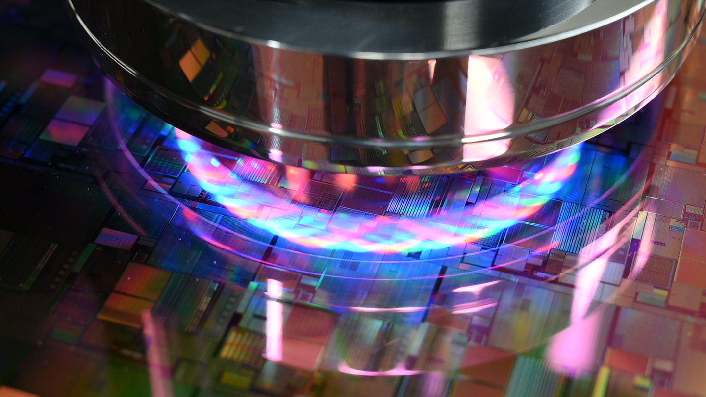
Wafer metrology refers to the precise measurement and analysis of semiconductor wafers used in the manufacturing of integrated circuits (ICs) and other electronic devices. It involves assessing various characteristics of wafers, such as dimensions, surface morphology, and material properties, using specialized techniques and instruments.
Importance of Wafer Metrology
Introduction
Optical measurement plays a critical role in modern precision manufacturing. Engineers constantly evaluate whether 2D or 3D optical measurement better suits their inspection needs. While both approaches rely on non-contact metrology, their capabilities, data output, and application suitability differ significantly. Understanding these
CMM calibration is not just a routine quality task. It is the foundation of reliable dimensional measurement. When accuracy matters, calibration defines confidence.
Introduction
Micro-fabricated parts are everywhere in modern manufacturing, yet they are rarely visible to the naked eye. As components become smaller, inspection becomes harder. Micro-fabricated part inspection exists to ensure these tiny parts meet design intent, function reliably, and comply with quality standards across manufacturing facilities.