


- Home
- Companies
- Wuhan Michuang Technology Co., Ltd ...
- Products
- MCscope - Model MC-TZG-4KCpro - 1000X ...
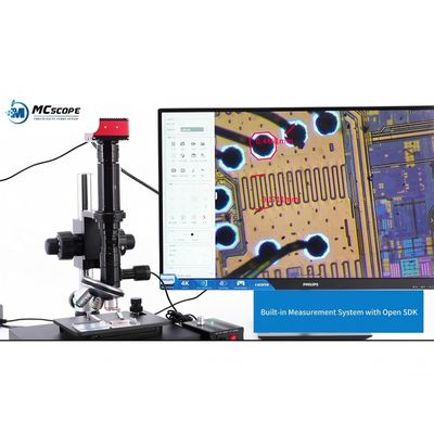
MCscope - Model MC-TZG-4KCpro -1000X Semiconductor Inspection Microscope
Specification Details
Optical Magnification: 0.7X–120X (with objective lens switching)
Electronic Magnification: 160X–4200X
Resolution: 3840 × 2160P @ 60FPS (4K UHD)
Camera Pixel: 8 Megapixels
Camera Output Interface: HDMI + USB 3.0 + Gigabit Ethernet port
External Devices: High-definition HDMI display + Computer
Auxiliary Objective Lens: Switchable metallurgical objectives (5X, 10X, 20X)
5X Objective: NA 0.12, WD 23.6mm, Resolution 2.8μm
10X Objective: NA 0.25, WD 17.7mm, Resolution 1.34μm
20X Objective: NA 0.40, WD 10.4mm, Resolution 0.8μm
Coarse and Micro Focusing: Fine adjustment value 0.002mm, focusing stroke 50mm
Mobile Platform: XY-axis dual-layer mechanical stage 187mm × 160mm; mobile range 60mm × 55mm
Camera Functions: Automatic edge finding, secondary development support, two/four screen comparison, magnification display, electronic zoom in/out, built-in measurement system, U disk storage
Visit more MCsocpe semiconductor inspection solutions.
1. Semiconductor Inspection
Designed for detailed inspection of semiconductor components such as wafers, ICs, and bonding structures. Enables observation of micro-scale features, surface defects, and fine structural details critical to device performance.
2. PCB & Microelectronics Inspection
Suitable for high-magnification inspection of PCB traces, pads, and micro-components. Helps identify fine defects such as micro-cracks, poor solder joints, and surface contamination in advanced electronics.
3. IC Packaging & Wire Bond Inspection
Used to examine wire bonding, chip packaging, and interconnection quality. Supports detection of bonding defects, misalignment, and structural inconsistencies at high magnification.
4. Material Surface & Microstructure Analysis
Enables detailed analysis of material surfaces, coatings, and microstructures. Ideal for identifying scratches, grain structures, and micro-level defects in metals and advanced materials.
5. Precision Component Inspection
Applied in the inspection of ultra-small mechanical and electronic components. Ensures dimensional accuracy, surface quality, and structural integrity in precision manufacturing.
6. Research & Laboratory Analysis
Suitable for laboratory environments requiring high-magnification imaging and documentation. Supports detailed observation, image capture, and analysis of micro-scale samples in research applications.