Alphacen - Model 200 Drive -Advanced Atomic Force Microscope (AFM) System
Based on our expertise designing industrial metrology systems, Nanosurf developed the Alphacen 200 Drive – an advanced AFM system engineered to meet the high demands of the semiconductor industry. From unparalleled low-noise roughness analysis using WaveMode to complex electrical characterization tasks with SMM, the Alphacen 200 Drive solves the challenges typically faced by semiconductor manufacturing and research.
- Large sample system with flexure tip scanner capable of atomic resolution.
- Highest measurement stability with CleanDrive photothermal excitation.
- WaveMode: Fastest off-resonance imaging for reproducible and fast measurements.
- Large scan range: 100 x 100 x 20 μm³.
- Compatible with broad selection of nanoelectrical characterization methods (NEC), such as Nanosurf’s SMM solution.
- Expandable functionality with accessories and software options.
- Fully automated laser alignment and cantilever calibration.
- Automated imaging on every region of interest within fully addressable XY sample area of 200 x 200 mm².
- Accurate and consistent roughness measurements with WaveMode.
Thanks to the superior technology of the DriveAFM scan head, imaging at atomic resolution is possible, even on this large-stage system.
This powerful combination allows for the observation of feature sizes covering several orders of magnitude, making a wide variety of structures accessible for analysis.
- Obtain local capacitance, carrier density, resistance, conductivity, and dielectric constant.
- Analyze sub-surface structures prevalent in modern multilayered integrated circuits.
- Fastest time-to-results with Nanosurf’s in-house SMM solution.
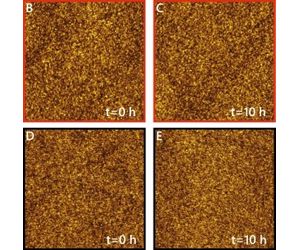
A) Time series of 10 h continuous RMS surface roughness measurements on a silicon wafer using WaveMode (WM) off-resonance tapping (red) and non-contact dynamic mode (NC) using CleanDrive photothermal excitation (black). The average surface roughness (±SD) correspond to 172±2 pm and 100±4 pm, respectively. First and last images of the WM (B, C) and NC mode (D, E) measurement series. Image size: 1 x 1 μm²; full z color scale: 1 nm (WM) and 0.7 nm (NC). All images were recorded at 5 Hz line rate with 500 px x 500 px resolution using WM0.6AuD (WM, 70 pN contact force) or USC-F1.2-k7.3 (NC, 2.8 nm free amplitude, 87% setpoint) cantilevers.