
- Home
- Equipment
Refine by
Svm Xprt Equipment & Supplies
23 equipment items found
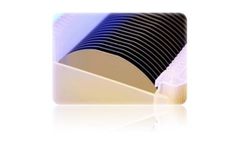
Distributed by:Silicon Valley Microelectronics, Inc. (SVM) based inSanta Clara, CALIFORNIA (USA)
SVM’s product line includes both single side polished (SSP) and double side polished (DSP) wafer substrates. Double side polished wafers are typically required in semiconductor, MEMS, and other applications where wafers with tightly controlled flatness characteristics are required. They are also needed for double side patterning and device manufacturing ...
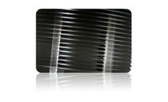
Distributed by:Silicon Valley Microelectronics, Inc. (SVM) based inSanta Clara, CALIFORNIA (USA)
SVM supplies Thick Wafers in all diameters (50mm to 300mm), with thickness specifications up to and greater than 2 mm. Surface finish can be lapped, etched, or polished. SVM will custom manufacture wafers to your exact thickness ...

Distributed by:Silicon Valley Microelectronics, Inc. (SVM) based inSanta Clara, CALIFORNIA (USA)
Solar cells that are created from mono-crystalline or (single crystal) technology are cut from a silicon ingot that is grown from a single crystal, in other words, a crystal that has grown in only one plane or (one direction). Mono-crystalline are more expensive to manufacture and typically have a slightly higher efficiency than do conventional poly-crystalline ...
Distributed by:Silicon Valley Microelectronics, Inc. (SVM) based inSanta Clara, CALIFORNIA (USA)
Solar grade virgin polysilicon is distinguished by its purity. Solar grade virgin polysilicon generally falls between the levels of “6 nines” to “9 nines” of purity. This means that the solar grade virgin poly is % 99.9999 pure or ...
Distributed by:Silicon Valley Microelectronics, Inc. (SVM) based inSanta Clara, CALIFORNIA (USA)
Ingots are grown through a process known as Czochralski (CZ) method. CZ ingot growth requires chunks of virgin polycrystalline silicon which are placed in a quartz crucible along with small quantities of elements called dopants – the most common of which are boron, phosphorus, arsenic and antimony. The materials are heated to a temperature above the melting point of silicon, 1420 degrees ...

Distributed by:Silicon Valley Microelectronics, Inc. (SVM) based inSanta Clara, CALIFORNIA (USA)
SVM carries a full line of 50mm wafers. Please see below a SEMI standard specification for prime and test grade wafers. Every customer’s specification is unique and SVM can supply wafers that meet your exact ...
Distributed by:Silicon Valley Microelectronics, Inc. (SVM) based inSanta Clara, CALIFORNIA (USA)
SVM supplies a wide variety of high quality lithography grade Silicon Wafers to meet your exact controlled flatness requirements. Wafer diameters available: 50mm to 300mm. Flatness measurement available: SFPD, SFQR, STIR, TTV, TIR, GTIR ...
Distributed by:Silicon Valley Microelectronics, Inc. (SVM) based inSanta Clara, CALIFORNIA (USA)
SVM carries a full line of 125mm wafers. Please see below a SEMI standard specification for prime and test grade wafers. Every customer’s specification is unique and SVM can supply wafers that meet your exact ...
Distributed by:Silicon Valley Microelectronics, Inc. (SVM) based inSanta Clara, CALIFORNIA (USA)
SVM carries a full line of 150mm wafers. Please see below a SEMI standard specification for prime and test grade wafers. Every customer’s specification is unique and SVM can supply wafers that meet your exact ...

Distributed by:Silicon Valley Microelectronics, Inc. (SVM) based inSanta Clara, CALIFORNIA (USA)
Lithography Grade Wafers are substrates that have tightly controlled flatness characteristics. These wafers will be manufactured with very flat Total Thickness Variance (TTV) specifications and site flatness measurements providing little variation in surface flatness within the site ...
Distributed by:Silicon Valley Microelectronics, Inc. (SVM) based inSanta Clara, CALIFORNIA (USA)
Growing a silicon ingot can take anywhere from one week to one month, depending on many factors, including size, quality and specifications. More than 75% of all single crystal silicon wafers are grown using the Czochralski (CZ) method. CZ ingot growth requires chunks of virgin polycrystalline silicon. These chunks are placed in a quartz crucible along with small quantities of elements called ...
Distributed by:Silicon Valley Microelectronics, Inc. (SVM) based inSanta Clara, CALIFORNIA (USA)
Float Zone (FZ) silicon is commonly used in the manufacture of discrete power devices, high efficiency solar, RF chips and optical products. FZ silicon is a high purity alternative to Czochalski (CZ) grown silicon whereas the concentration of carbon and oxygen impurities are extremely low. The purity of FZ allows the silicon to go through a lighter doping process, sometimes producing resistivity ...
Distributed by:Silicon Valley Microelectronics, Inc. (SVM) based inSanta Clara, CALIFORNIA (USA)
Most commonly used in MEMS and advanced CMOS integrated circuit fabrication, SOI wafers provide a manufacturing solution which helps reduce power and heat while increasing the speed performance of a device. SOI wafers are a three layer material stack composed of the following: Active layer of prime quality silicon (DEVICE LAYER) over a buried layer(BOX) of electrically insulating silicon dioxide, ...
Distributed by:Silicon Valley Microelectronics, Inc. (SVM) based inSanta Clara, CALIFORNIA (USA)
Semi conductor grade virgin polysilicon is distinguished by its extraordinary purity. Semiconductor grade virgin poly generally reaches levels of “11 nines” or “12 nines of purity”, thus, semiconductor grade virgin poly is 99.9999999999 percent pure or ...
Distributed by:Silicon Valley Microelectronics, Inc. (SVM) based inSanta Clara, CALIFORNIA (USA)
Tops and Tails are derived from a fully-grown polysilicon ingot. Once fully grown, an ingot is removed from the quartz crucible from which it was pulled. Because the ingot was pulled at various speeds during growth, the ends are narrower than the silicon body. The narrow sections of the ingot are removed from the cylindrical body. These ends can be re-melted and used again in the growing ...
Distributed by:Silicon Valley Microelectronics, Inc. (SVM) based inSanta Clara, CALIFORNIA (USA)
SVM supplies Thin Silicon Wafers in wafer diameters ranging from 50mm to 300mm. For high volume requests, Thin Wafers are manufactured to customer unique specifications. For smaller volume projects, precision BACK GRINDING, LAPPING and POLISHING work is applied to an SVM stock wafer specification which has been manufactured to SEMI standard thickness. SVM provides thin substrates starting from a ...
Distributed by:Silicon Valley Microelectronics, Inc. (SVM) based inSanta Clara, CALIFORNIA (USA)
SVM carries a full line of 76mm wafers. Please see below a SEMI standard specification for prime and test grade wafers. Every customer’s specification is unique and SVM can supply wafers that meet your exact ...
Distributed by:Silicon Valley Microelectronics, Inc. (SVM) based inSanta Clara, CALIFORNIA (USA)
SVM carries a full line of 100mm wafers. Please see below a SEMI standard specification for prime and test grade wafers. Every customer’s specification is unique and SVM can supply wafers that meet your exact ...
Distributed by:Silicon Valley Microelectronics, Inc. (SVM) based inSanta Clara, CALIFORNIA (USA)
Test Grade Wafers are high quality wafers which have less comprehensive specifications than a prime grade wafer. These wafers monitor the performance and conditions of a particular semiconductor processing step. The Test Grade Wafer provides a more economical solution for isolated ...
Distributed by:Silicon Valley Microelectronics, Inc. (SVM) based inSanta Clara, CALIFORNIA (USA)
Low Resistivity Wafers, commonly referred to as P+ and N+ wafers, are heavily doped substrates that produce highly conductive, very low resistivity characteristics. SVM has a large inventory of P+ and N+ wafers available in all ...