

- Home
- Companies
- Angstrom Engineering Inc.
- Products
- Angstrom Engineering - Linear Sputter ...
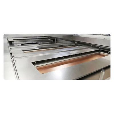
Angstrom Engineering - Linear Sputter PVD System
Using the Linear Sputter PVD system from Angstrom Engineering allows you to process thin films of semiconductors or metals on large area panels in display, photovoltaic, and semiconductor applications. We designed these systems to address the challenges researchers face when sputtering over large areas or quantities of substrates. From gas flow and plasma management to magnetron uniformity and temperature control, Angstrom Engineering®’s Linear Sputter PVD systems let you revolutionize your workflow and see higher throughput production than previously possible. Create devices on very large substrates, stacking multiple layers in a single run with great uniformity. Even though the targets are larger than usual, the material is very efficiently utilized.
- PC/PLC-controlled recipes for single, batch, or automated processes.
- Advanced data logging and process tracking ensure consistent and repeatable processes.
- High-resolution control provides impressive low-rate stability and consistent doping ratios.
- The central control station manages each module and schedules the processes in each chamber.
- Independent control of multiple chambers (if applicable).
- Complex recipes can be created and modified easily.
- Automatic PID control loop tuning significantly reduces process development time.