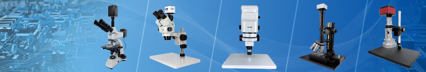

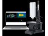
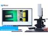
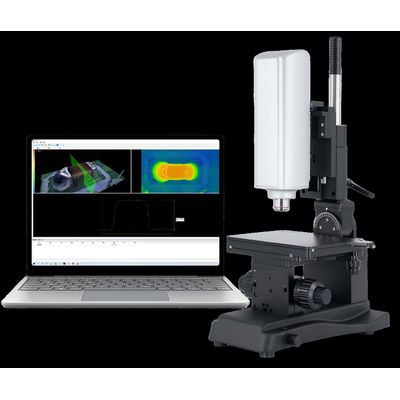
MCscope - Model MC-HX2000 -3D Measuring Microscope
- High-Precision 3D Measurement – Supports 2D & 3D analysis, multi-profile height mapping, and automatic edge detection.
- Extended Depth-of-Field (EDF) – Focus stacking maintains sharp images across uneven or multi-height surfaces.
- Multi-Angle XY & Tilt Observation – ±90° tilt and motorized/optional XY stage for complex geometries.
- Automated Zoom & Calibration – Motorized zoom with auto magnification switching and calibration for workflow consistency.
- Hybrid Brightfield & Darkfield Illumination – Customizable lighting ensures uniform contrast on reflective surfaces.
- Report & Workflow Integration – Export measurement data and maintain focus during lens tilting.
- 0.1 μm XY Resolution – High-precision positioning for micron-level measurement.
- Multi-angle observation for complex geometries
Model: MC-HX2000
Microscope Type: 3D High-Depth Measuring Microscope
Zoom Type: Motorized Variable Magnification
Optical Zoom Ratio: 1:6.5
Electronic Magnification: 270X – 1700X
Objective Lens: Standard 10X (Optional: 5X / 20X / 50X)
Spatial Resolution: 2.0 × 2.0 μm
Image Sensor Size: 1/1.8″
Output Interface: HDMI + Gigabit Ethernet
Lens Tilt Angle: -90° to +90°
Stage Travel (X / Y): 100 mm × 100 mm
Z-axis Motorized Travel: 50 mm
Maximum Sample Height: 220 mm
Illumination System: Brightfield & Darkfield Combined
2D Measurement Functions: Point, Line, Area
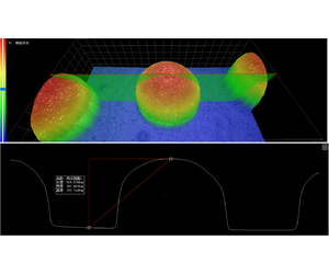
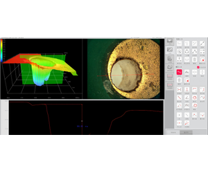
3D Profile Measurement: Depth & Irregular Groove Height
Extended Depth-of-Field (EDF): Supported
Image Stitching: Supported
3D Surface Modeling: Supported
Measurement Data Management: Template Import & Report Storage
Camera Functions: Image Capture, High-Precision Measurement, Image Composition
Typical Applications: 2D/3D Measurement, Height Analysis, 3D Surface Profiling
1. Electronics & PCB Inspection1. Electronics & PCB InspectionPerform accurate measurement of solder joints, IC packages, connectors, and PCB features. Measuring microscopes help verify critical dimensions, coplanarity, spacing, and height differences that directly affect assembly quality and product reliability.
2.Precision Manufacturing & MachiningMeasure groove depth, step height, edge geometry, and precision-machined features. Non-contact dimensional analysis helps engineers improve machining accuracy, reduce tolerances, and verify complex part geometries.
3.Semiconductor & Advanced PackagingMeasure wafer features, chip dimensions, package structures, and surface topography. Measuring microscopes support accurate dimensional verification and height analysis for semiconductor manufacturing and advanced packaging processes.
4.Materials Science & MetallographyAnalyze grain structures, coating thickness, surface profiles, and material defects. Quantitative measurement capabilities help researchers compare material characteristics and evaluate manufacturing consistency.
5.Quality Control & Metrology LabsPerform routine dimensional verification, process control measurement, and inspection documentation. Measurement software enables traceable data collection, reporting, and long-term quality monitoring.
6.Micro-Mechanical Parts & Precision Component InspectionMeasure hole diameters, groove widths, edge profiles, and micro-scale features with high accuracy. Non-contact measurement helps inspect delicate components that are difficult to evaluate using conventional tools.