


Semilab Semiconductor Physics Laboratory Co. Ltd.
- Home
- Companies
- Semilab Semiconductor Physics ...
- Products
- SEMILAB - Model WT-2000 - Multifunction ...
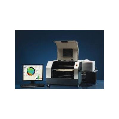
SEMILAB - Model WT-2000 -Multifunction Wafer Mapping Tool
The WT2000 is a tabletop tool, suggested for mid-range fabs and laboratories.
Most popular related searches
wafer thickness
contamination monitoring
contaminant monitoring
thermal oxidation
heavy metals
thermal oxidizer
mapping system
wafer thickness measurement
heavy metals monitoring
heavy metals contamination
- Wafer size: up to 300 mm with bare or dielectric coated surface
- Wafer handling: manual or Semilab made indexer
- Loading options:
- 100-200 mm cassette indexer
- 300 mm 13-slot cassette indexer, including open cassettes for 100-300 mm wafers
- 300 mm 25-slot cassette indexer, including FOUP, FOSB, and open cassettes for 100-300 mm wafers
- Objectives of detection:
- Impurities due to heavy metal and transition metal contamination
- Crystal defects
- Optional iron concentration determination both in CZ and FZ wafers
- No wafer thickness limitation
- Fast measurement speed
- High lateral resolution
- Required surface passivation: thermal oxide, chemical passivation or corona charging