
Refine by
Optical Metrology System Articles & Analysis
39 articles found

Shrinking wire diameters, combined with material variability across aluminum and copper to gold and palladium coated alloys, have increased inspection complexity, particularly for measuring wire loop geometry, electrical continuity, and bond placement on highly-reflective surfaces. Conventional optical inspection systems often struggle to resolve the tops of ...
If we look around at today’s electronics things are getting smaller day by day but power and performance are only going up. Phones laptops cars even small IoT devices all need to do more work in less space. That is where packaging starts to matter a lot. QFN packaging came in as a practical solution when this shift started happening. It helped engineers manage space without losing ...
In today’s era of miniaturized, high-performance electronics, the true effectiveness of a semiconductor chip (die) depends not only on its design—but on its packaging. While the chip’s performance is crucial, it is the semiconductor packaging that enables functional integration, protects device integrity, and ensures reliable connections within microelectronic systems. As form ...
What is Wafer Metrology? Wafer metrology refers to the precise measurement and analysis of semiconductor wafers used in the manufacturing of integrated circuits (ICs) and other electronic devices. It involves assessing various characteristics of wafers, such as dimensions, surface morphology, and material properties, using specialized techniques and instruments. Importance of Wafer Metrology ...
Introduction Optical measurement plays a critical role in modern precision manufacturing. Engineers constantly evaluate whether 2D or 3D optical measurement better suits their inspection needs. While both approaches rely on non-contact metrology, their capabilities, data output, and application suitability differ significantly. Understanding these differences helps improve accuracy, efficiency, ...
The measurement of manufactured components has evolved across decades. Traditional coordinate measuring machines (CMM) set a foundation for precision validation, while optical metrology introduced speed and non-contact ...
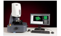
The aerospace industry operates at the outer limits of engineering possibility. Every component (whether a turbine blade, flight control sensor, or optical window) must deliver flawless performance in extreme conditions of heat, stress, and vibration. In such an environment, even the smallest deviation can result in inefficiency, downtime, or catastrophic failure. For more than 50 years, ...
Introduction A measurement system is something we depend on every day, even if we never think about it. From checking the length of a part to ensuring a product meets tight tolerances, measurements guide decisions. In this guide, we will explore measurement systems ...
A profilometer is a precision instrument used to measure the surface profile of objects, providing critical insights into surface roughness, texture, and step height. For anyone working in industries requiring high accuracy, understanding profilometers is essential. This guide explains everything about profilometers, from basic principles to industrial applications. ...
Introduction Ever wondered how machines “know” when an object is nearby without touching it? Inductive proximity sensors are behind this magic in factories, electronics, and automation. They detect metal objects without contact and are critical in precision operations, quality control, and safety. This blog explores how these sensors work, the different types, and their ...
Introduction Ever wondered how machines “know” when an object is nearby without touching it? Inductive proximity sensors are behind this magic in factories, electronics, and automation. They detect metal objects without contact and are critical in precision operations, quality control, and safety. This blog explores how these sensors work, the different types, and their ...
Semiconductor chip packaging is the final yet most critical stage in the semiconductor manufacturing chain, where a fabricated silicon die is transformed into a usable component for electronic devices. While the integrated circuit itself may contain billions of transistors, it cannot function in a system without proper packaging. Packaging provides mechanical protection, electrical ...
What Is Heterogeneous Integration? Heterogeneous Integration refers to the process of combining multiple types of components, such as logic chips, memory, sensors, photonics, and RF modules, into a single compact system. These components are often manufactured using different materials and processes, but are combined into a unified package to deliver advanced functionality and high-performance ...
In the era of miniaturized, high-performance electronics, the semiconductor chip is only as effective as its packaging. While the spotlight often falls on the chip itself, it is the semiconductor packaging that enables integration into real-world systems. This article by View Micro Metrology breaks down the concept of semiconductor packaging to help you understand what it is, why it matters, how ...

Fan-Out Wafer Level Packaging (FOWLP) has emerged as a game-changer in semiconductor packaging. It enables chips to be packaged with more I/O (input/output) density, superior electrical performance, and reduced size, meeting the needs of industries like 5G, automotive, AI, and consumer ...
In the era of nanotechnology and semiconductor advancement, photomasks serve as a cornerstone in the microfabrication process. These precision-engineered optical templates are crucial to lithography-based patterning, which defines the microstructures in integrated circuits, MEMS, and other micro-scale devices. Understanding photomasks and their role provides insight into how precision and ...
Laser metrology is a subfield of optical metrology that utilizes the unique properties of laser light—coherence, monochromaticity, and low divergence—for precise distance, angle, and dimensional measurements. Instead of physical probing, lasers capture measurements safely and quickly—especially useful for intricate or lightweight items. At its core, laser metrology is about ...
In modern manufacturing and engineering, precision is more than a goal—it’s a necessity. Whether producing aerospace components, medical devices, or semiconductor chips, manufacturers must ensure every part conforms to tight tolerances and quality control standards. This is where industrial metrology plays a crucial ...
Semiconductor metrology is a specialized branch of measurement science that ensures the accuracy and precision of semiconductor manufacturing processes. The evolution of semiconductor technology, from early microprocessors to today’s highly advanced integrated circuits (ICs), has been driven by the demand for smaller, faster, and more efficient electronic devices. As semiconductor ...
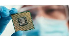
Manufacturing has become the backbone of all types of industries in the world, before reaching the customer’s hands every product is tried and tested to a high degree. Behind every good product you use lies a quality control process that makes sure the products meet the highest standards. If there’s a lack of quality control in manufacturing, even the most innovative designs can ...