
Refine by
Semiconductor Wafer Articles & Analysis
45 articles found

With stable system operation and strong anti-fluctuation capability, it supports uninterrupted mass production and ensures long-term stable compliance with emission standards.Scenario 2: Vehicle-Grade Chip & Semiconductor Exhaust Gas Treatment — High-End Environmental Requirements for Clean Manufacturing With the rapid iterative upgrading of intelligent vehicles, ...

VOC Characteristics and Treatment Cases in the Semiconductor & Electronics Industry The semiconductor and electronics industry involves highly complex processes such as cleaning, photolithography, developing, and stripping, resulting in diverse and sophisticated VOC emissions. Main Pollutants Acetone Isopropanol PGME PGMEA NMP This industry requires ...
In packaging and printing (film composite and gravure printing), it handles ethyl acetate, IPA and toluene, achieving 97%-99% recovery rate. For semiconductor wafer cleaning and photoresist processes, it purifies PGMEA, PGME, IPA and acetone with efficiency over 97%. ...
As the 3C electronics manufacturing industry continues to expand globally, VOC emissions from production processes have become an increasingly critical environmental challenge. From semiconductor wafer fabrication to consumer electronics enclosure manufacturing, each production stage generates complex volatile organic compounds (VOCs) with varying concentrations ...

What is Wafer Metrology? Wafer metrology refers to the precise measurement and analysis of semiconductor wafers used in the manufacturing of integrated circuits (ICs) and other electronic devices. It involves assessing various characteristics of wafers, such as dimensions, surface morphology, and material ...
Introduction Optical measurement plays a critical role in modern precision manufacturing. Engineers constantly evaluate whether 2D or 3D optical measurement better suits their inspection needs. While both approaches rely on non-contact metrology, their capabilities, data output, and application suitability differ significantly. Understanding these differences helps improve accuracy, efficiency, ...
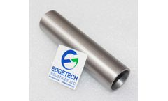
Table of contents: How Tungsten Tubes Are Revolutionizing Semiconductor Manufacturing The Role of Tungsten Tubes in Medical Devices and Equipment Why Tungsten Tubes Are Essential in Nuclear Energy Applications This blog post aims to shed light on how tungsten tubes are revolutionizing sectors like semiconductor manufacturing, medical devices, and nuclear ...
The measurement of manufactured components has evolved across decades. Traditional coordinate measuring machines (CMM) set a foundation for precision validation, while optical metrology introduced speed and non-contact ...

The chemistry of a material’s outermost nanometres often determines its functional performance, making accurate surface characterisation vital for modern materials research. Yet, analysing these nanometre-scale layers is inherently challenging, as many surface-sensitive chemistry techniques, like AES, can modify the material or disturb its native chemical composition and techniques like EDX ...
Introduction Surface finish tells us a lot about how a part will perform, whether it will seal properly, move smoothly, or wear too soon. Measuring surface roughness is the science of quantifying those tiny peaks and valleys on a material’s surface. Over the years, this field has evolved from contact-based tools to advanced non-contact optical metrology techniques that deliver microscopic ...
Introduction Surface finish tells us a lot about how a part will perform, whether it will seal properly, move smoothly, or wear too soon. Measuring surface roughness is the science of quantifying those tiny peaks and valleys on a material’s surface. Over the years, this field has evolved from contact-based tools to advanced non-contact optical metrology techniques that deliver microscopic ...
Introduction If you’ve ever wondered how engineers measure the tiniest details on a surface from semiconductor wafers to mobile phone parts, the answer often lies in a field called profilometry. ...
In the era of nanotechnology and semiconductor advancement, photomasks serve as a cornerstone in the microfabrication process. These precision-engineered optical templates are crucial to lithography-based patterning, which defines the microstructures in integrated circuits, MEMS, and other micro-scale devices. Understanding photomasks and their role provides insight into how precision and ...

Accurate temperature measurement is critical across a wide range of industries, from manufacturing and energy production to semiconductor wafer furnaces. However, the performance of a temperature reading is directly tied to its accuracy. ...
Laser metrology is a subfield of optical metrology that utilizes the unique properties of laser light—coherence, monochromaticity, and low divergence—for precise distance, angle, and dimensional measurements. Instead of physical probing, lasers capture measurements safely and quickly—especially useful for intricate or lightweight items. At its core, laser metrology is about ...

Micrel owns a 150mm fab with a capacity of 30,000 wafer starts per month. The fab was constructed in the 1980s and is considered a legacy fab without the full benefits of current automation technology. The company constantly assesses technology upgrades to reduce cost and improve productivity in order to keep their competitive edge. Managing the use of process gases, which is labor intensive and ...

Gas delivery systems are fundamental to the semiconductor manufacturing process, where precision, safety, and efficiency are paramount. These systems enable meticulous control over the flow and composition of gases, which are crucial for processes like etching, doping, and deposition. Let’s dig into the role of gas delivery systems in semiconductor ...

Ensuring Cleanliness and Product Quality Keeping precision parts free from contamination is crucial in industries like aerospace, automotive, semiconductors, and medical devices. Even the smallest particles can impact performance, reduce product lifespan, or, in the case of medical implants, pose serious health risks. To maintain high cleanliness standards, manufacturers use strict cleaning ...

Ensuring Cleanliness and Product Quality Keeping precision parts free from contamination is crucial in industries like aerospace, automotive, semiconductors, and medical devices. Even the smallest particles can impact performance, reduce product lifespan, or, in the case of medical implants, pose serious health risks. To maintain high cleanliness standards, manufacturers use strict cleaning ...
Semiconductor metrology is a specialized branch of measurement science that ensures the accuracy and precision of semiconductor manufacturing processes. The evolution of semiconductor technology, from early microprocessors to today’s highly advanced integrated circuits (ICs), has been driven by the demand for smaller, faster, and more efficient electronic devices. As semiconductor ...