
Semilab Semiconductor Physics Laboratory Co. Ltd.
- Home
- Companies
- Semilab Semiconductor Physics ...
- Products
- Semilab - Model AFM-2200 - Atomic Force ...
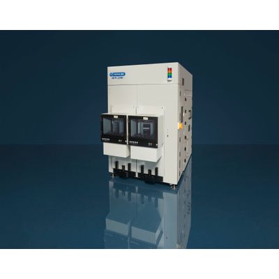
Semilab - Model AFM-2200 -Atomic Force Microscope
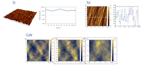
Semilab Atomic Force Microscopes provide high-resolution, sub-atomic precise measurements with extremely low noise level which enables consistent and highly reproducible roughness characterization for the quality control of Si and compound wafers. The Semilab AFM-2200 offers highly reproducible roughness characterization for the quality control of up to 12” semiconductor wafers for those seeking atomic force microscopy with an automated sample loading system.
Most popular related searches
atomic force microscopy
atomic microscopy
AFM tip
laser alignment
autosampling
microscopy
sample automation system
process analysis
sample automation
alignment laser
The Semilab AFM-2200 system is designed for various applications, including:
- CMP Process Control:
- Analysis of micro-roughness and lateral surface structures
- Automated Defect Review:
- Defect detection by light-scattering method (μPIT) and characterization using AFM
- Device Characterization:
- Critical Dimension measurements, failure analysis
- AFM Tip Scanner, utilizing flexure-guided piezo positioners for flat scanner movement
- Fully automated AFM with automatic simple loadport
- Automatic tip exchange and laser alignment
- Sub-atomic resolution
- Maximum scan area size can be configured according to industry requirements
- Full 12 inch wafer is accessible by the AFM scanner
- KLARF file import & export
- Profilometer mode
- Optional Advanced Defect Review and Pattern Recognition