


Semilab Semiconductor Physics Laboratory Co. Ltd.
- Home
- Companies
- Semilab Semiconductor Physics ...
- Products
- Semilab - Model AFM-1000 - Atomic Force ...
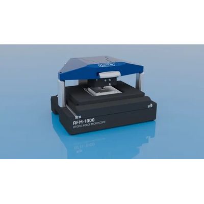
Semilab - Model AFM-1000 -Atomic Force Microscopy
The AFM-1000 from Semilab is a versatile atomic force microscope designed for both academic research and semiconductor industry applications. This compact system offers high-resolution, sub-atomic precision measurements with extremely low noise levels, ideal for consistent nanotopography measurements and electrical characterization of various samples up to 65x65 mm in size. With cutting-edge technology and decades of knowhow, Semilab tabletop AFM system provides to your academic research microscopic measurement solutions based on semiconductor industry standards.
Most popular related searches
atomic force microscopy
atomic microscopy
compaction system
microscopy
sample holder
electrical characterization
material science
research microscope
laser alignment
metrology
- Designed for R&D use: Materials science, semiconductor device research, advanced metrology
- Wide sample compatibility for various research applications
- Proven track record of Semilab AFM product family: Cited in multiple scientific publications
- AFM scanner utilizing flexure-guided piezo positioners for flat scanner movement
- Configurable scan area size
- Integrated dual focus camera system for laser alignment and tip-to-sample positioning
- Compact tabletop AFM system with small footprint for R&D applications
- Easy and safe sample and cantilever handling
- Manually adjustable laser path
- Motorized sample stage
- Sample holder: clamps or magnetic fixing
- High level of automation: series of different measurements can be automatically carried out on a single sample
Scan area customization options:
- Option 1
- Scan range: 50x50 µm
- Z range 5 µm
- Stage range: 20x20 mm
- Option 2
- Scan range: 100x100 µm
- Z range 10 µm
- Stage range: 20x20 mm