


Semilab Semiconductor Physics Laboratory Co. Ltd.
- Home
- Companies
- Semilab Semiconductor Physics ...
- Products
- Semilab - Model COREMA-2000 - ...
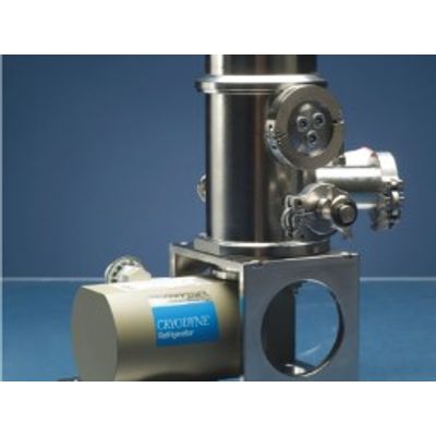
Semilab - Model COREMA-2000 -Contactless Resistivity Mapping
The COREMA-2000 series offers precise, non-destructive, contactless resistivity measurement solutions designed primarily for semi-insulating compound semiconductors such as SiC, GaN, GaAs, CdTe, GaO, and InP. It supports both research and industrial semiconductor manufacturing environments with high accuracy and repeatability.
Most popular related searches
real-time process monitoring
non-destructive measurement
non-destructive monitoring
resistivity profiling
process monitoring
optoelectronic
surface sampling
surface sample
- Resistivity mapping and uniformity assessment of compound semiconductor wafers before chip fabrication
- Quality control of incoming wafers in semiconductor production lines
- Real-time process monitoring of high-resistivity substrates in RF, optoelectronics, photonics, military, aerospace, and power device manufacturing
- Applicable to materials such as GaAs, SiC, GaN, GaO, CdTe, InP, and other semi-insulating substrates
- Original developer of the SEMI standard and leading global support network
- Fully compliant with SEMI M87-0422 industry standard for non-contact resistivity measurement
- Trusted and deployed globally in 14+ countries
- No calibration needed for routine operation
- User-friendly graphical interface with colored topographic display
- Non-contact, non-destructive full-wafer resistivity measurement
- Excellent measurement repeatability and wide measurement range
- Measurement Principle: Contactless capacitance technique for full-water resistivity characterization across a very wide range in the semi-insulating region
- Operator & Automation:
- Full automation supported on request (especially Corema-2201 model with robotic wafer handling)
- Measurement parameters and process sequences fully customizable
- Semi-automatic wafer placement
- Data & Software:
- Built-in software provides detailed wafer maps and resistivity profiles
- Customizable reporting tailored to industry standards with data available in various formats; Semilab internal format, TXT, and PDF
- Excellent repeatibility, <1%* (*:get in touch for further details),
- Sample Surface: Etched or polished, as-cut or bare wafer,
- Sample size up to 200 mm diameter,
- Minimum sample size: 10 x 10 mm shard for single point measurement,
- Wide measurement range: 105to 10¹² Ω·cm
- Measurement parameters:
- Full wafer topogram with up to 1024x1024 data points
- Fast evaluation
- Wafer diameter: up to 200 mm
- Manual wafer handling
- Automatic non-contact adjustment
- Mapping capability