
Refine by
Applications
- Process analyzers & instruments for thin film/semiconductor/PVD
- Monitors, gas analyzers solutions for ISO 14644-1/2: 2015 insights & solutions
- Air quality and industrial gas monitoring systems for Semiconductor
- Measurements Solutions for Topography & Texture
- Measurements Solutions for Wedge & Prism Angle
- Measurements Solutions for Radius of Curvature
- Measurements Solutions for New Space Optics
- Measurements Solutions for Optics & Photonics
- Measurements Solutions for Research
- Measurements Solutions for Start Up
- Process analyzers & instruments for trace moisture
- Process analyzers & instruments for rack and benchmount
- Measurements Solutions for Semiconductor Industry
- Measurements Solutions for Aerospace
- Monitors, gas analyzers solutions for semiconductor / microelectronics sector
- Measurements Solutions for Automotive
- Measurements Solutions for Consumer Electronics
- Measurements Solutions for Defense
- Measurements Solutions for Asphere & Freeform Metrology
- Measurements Solutions for Roughness Metrology of Aspheres & Freeforms
- Measurements Solutions for Datum & Relational Metrology
- Environmental solutions for the pharmaceutical industry
- Monitors, gas analyzers solutions for photonics & optics
- Monitors, gas analyzers solutions for aerospace & defense industry
- Measurements Solutions for Commercial Space
- Measurements Solutions for Medical
- Flow Solutions for Original Equipment Manufacturers (OEM)
- Flow Meters for Food & Beverage Process Control
- Environmental solutions for the chemical processing industry
- Water treatment solutions for cooling water treatment
- Water treatment solutions for utility water treatment
- Process analyzers & instruments for trace carbon monoxide
- Process analyzers & instruments for trace carbon dioxide
- Process analyzers & instruments for trace hydrogen
- Process analyzers & instruments for trace methane
- Air quality and industrial gas monitoring systems for Medical, pharmaceutical, food & beverage
- Li-ion battery electrode manufacturing
- Environmental solutions for the printing and packaging industry
- Trace gas analyzers for ammonia in hydrocarbons applications
- Trace gas analyzers for hydrazine sector
- Nano-analytical microscope systems solutions for materials science sector
- Nano-analytical microscope systems solutions for pharmaceutics & cosmetics sector
- Nano-analytical microscope systems solutions for Life science sector
- Nano-analytical microscope systems solutions for geo science sector
- Nano-analytical microscope systems solutions for food technology sector
- Nano-analytical microscope systems solutions for semiconductors & photovoltaics sector
- Nano-analytical microscope systems solutions for nano-carbon & 2D materials sector
- Nano-analytical microscope systems solutions for polymers sector
- Nano-analytical microscope systems solutions for forensics sector
- Nano-analytical microscope systems solutions for archaeology & the arts sector
- Nano-analytical microscope systems solutions for coatings & thin films sector
- Plasma for Solar Technology
- High quality detection solutions for first response sector
- High quality detection solutions for public security sector
- High quality detection solutions for environment industry
- Monitors, gas analyzers solutions for food and beverage safety sector
- Trace gas analyzers for airborne molecular contamination (AMC) sector
- Air Pollution Measurements for Education
- Sensors for Air Quality Measurements?
- Multiprobes for Surface Water
- Multiprobes for Harmful Algal Bloom
- Multiprobes for Coastal
- Multiprobes for Stormwater
- Multiprobes for Aquaculture
- Multiprobes for Sourcewater
- Multiprobes for Groundwater
- Multiprobes for Dye Tracing
- Multiprobes for Dredging
- Multiprobes for Multiprobes for Dredging
- Multiprobes for Wastewater
- Multiprobes for Oil & Gas
- Multiprobes for Early Warning
- Measurements Solutions for Optical Material Homogeneity
- Measurements Solutions for Total Thickness Variation (TTV)
- Measurements Solutions for Optical Components
Semiconductor Equipment Supplied In Germany
516 equipment items found

Manufactured by:Heraeus Conamic based inKleinostheim, GERMANY
Heraeus Black Quartz (HBQ®) is a unique black opaque quartz glass composite that benefits from high purity and other properties of our advanced white opaque (OM®) and clear fused (HSQ®) quartz solutions. HBQ® offers smart answers to individual problems, and new answers to old material challenges. Convince yourself and step into a new world of possibilities with Heraeus Black ...
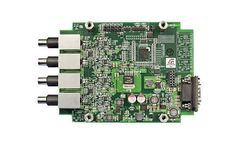
Manufactured by:Advanced Energy Industries, Inc. based inDenver, COLORADO (USA)
Advanced Energy's Luxtron four-channel m924 and two-channel m922 semiconductor modules are designed for etcher and wafer fab equipment temperature monitoring of electrostatic chucks, chambers, and other devices. Mix and match components. Works with current semiconductor Luxtron brand Fluoroptic probes and fiber optic extensions. ...
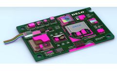
Manufactured by:DELO based inWindach, GERMANY
Adhesives are key components in semiconductor-based devices. DELO semiconductor adhesives are used to bond, contact and encapsulate chips and other SMD components on printed circuit boards. From RFID labels, MEMS sensors to optical components – DELO semiconductor adhesives are used wherever short cycle times and maximum precision are ...
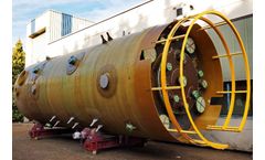
Manufactured by:Plasticon Composites GmbH based inStade, GERMANY
Plasticon Composites offers a wide range of vessels for the processing of chemicals; for example, columns, reactors, agitator vessels, settling tanks, gas coolers, scrubbers, absorbers and the related components and additional equipment. These components are designed in accordance with the dynamic and hydrostatic loads that occur in the different processes. They are used in various industries ...
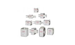
Manufactured by:Mersen based inPagny sur Moselle, FRANCE
Semiconductor protection fuses are used to protect against overcurrent conditions in power electronic equipment. They are specifically designed to reduce the I2t, peak let-through current and arc voltages during a fault ...

Manufactured by:Oxidkeramik J. Cardenas GmbH based inAlbershausen, GERMANY
OXIDKERAMIK J. Cardenas GmbH also uses ceramics to manufacture components for the semiconductor industry. All of the company's high-performance ceramics are used. We also manufacture insulators for electrical insulation from aluminum oxide ceramic OK997 ...
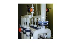
Manufactured by:ZIND Verfahrenstechnik based inMainz, GERMANY
The semiconductor market places the highest demands on media. In this high tech market, components for demanding products are produced under the purest conditions at high standards. This places high demands on the supplier in the areas of purity in production, quality management and cooperation with (reactions to) the customer/partner. ...
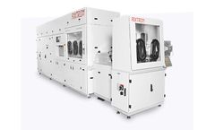
Manufactured by:Aixtron based inHerzogenrath, GERMANY
Key Benefits: Best Deposition Uniformity Control – at wafer level, Lowest Particle Count, Highest Product Yield, Lowest Production ...
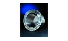
Manufactured by:Tosoh SMD, Inc. based inGrove City, OHIO (USA)
Tosoh offers Titanium targets for all major OEM PVD systems. Targets for all wafer sizes can be made in purities ranging from 3N to 5N+. Through control of the target metallurgy, oxygen content, surface finish and assembly technology, Tosoh offers titanium targets that light off easily, produce low particulate and provide consistent and repeatable thin ...
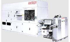
Manufactured by:Aixtron based inHerzogenrath, GERMANY
“Best performance for Next Generation SiC Power Electronics to address Global Mega Trends”. High throughput batch epitaxy with single wafer control - combining best of both worlds. Key Benefits: Best in class throughput and lowest cost of ownership per wafer, Single wafer performance in batch configuration for excellent epitaxial layer quality, Si fab compatible automation ...
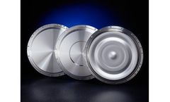
Manufactured by:Tosoh SMD, Inc. based inGrove City, OHIO (USA)
Tosoh SMD provides splat free Aluminum target material through a combination of our advanced metallurgy, assembly technology, high yield backing plates and nondestructive testing methods. Tosoh SMD determines the specific optimum aluminum grain size, crystal structure and chemical homogeneity necessary to achieve the best uniformity and film properties for a specific OEM system. Our optimized ...
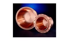
Manufactured by:Tosoh SMD, Inc. based inGrove City, OHIO (USA)
Copper is used for a variety of thin film applications including as a conductor material in logic and memory devices. Tosoh offers Copper targets for all major OEM PVD systems. Targets for all wafer sizes can be made in purities ranging from 4N to 6N. Through control of the target metallurgy, surface finish and assembly technology, Tosoh offers Copper targets that light off easily and provide ...
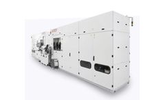
Manufactured by:Aixtron based inHerzogenrath, GERMANY
State-of-the-art Planetary reactor module for advanced GaN application on 150/200 mm substrates (Si/Sapphire/SiC) increases productivity and wafer performance. Key Benefits: Chosen by the best in the industry, Highest throughput, Lowest Cost of Ownership, Highest yield performance, 1st fully automated MOCVD platform with Cl2 in-situ cleaning and cassette-to-cassette wafer handler ...
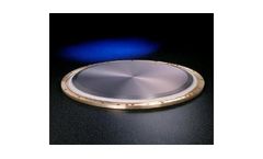
Manufactured by:Tosoh SMD, Inc. based inGrove City, OHIO (USA)
Tantalum is used for a variety of thin film applications: as a diffusion barrier material in logic, and memory devices, as a gate electrode in MOSFET devices and as a protective coating on print head devices. Tosoh offers a variety of Tantalum targets using OEM and Tosoh-modified designs for all major platforms. Purities ranging from 3N5 to 5N+ are available. Texture and grain size can be ...
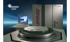
Manufactured by:Advantest America,Inc. based inSan Jose, CALIFORNIA (USA)
SoC devices require small-lot high-mix manufacturing methods in the present era of rapid generation change. Semiconductor makers struggle with requirements to replace their testers on a 2-3 year cycle. The T2000 addresses their needs by enabling rapid response to market needs with minimum capital ...

Manufactured by:NovaCentrix based inAustin, TEXAS (USA)
The PulseForge 3300 is designed to process higher melting point materials, such as silicon, zinc oxide, ITO, ceramics and CIGS, used for printed logic, display, and photovoltaic applications. The tools create the very high processing temperatures required for recrystallization and annealing, but without damaging low - temperature materials like polymeric substrates, glass (including thin flexible ...
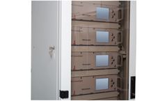
Manufactured by:IUT Technologies GmbH based inBerlin, GERMANY
With our solution, gaseous substances can be detected and identified without any enrichment directly in situ, already at a very low (ppt) concentration level. The detection including sampling and identification process takes minutes to seconds, depending on the configurated setup. ...

Manufactured by:WEDECO - a Xylem brand based inHerford, GERMANY
In the manufacturing of semiconductor elements the required ultrapure water plays a fundamental role. The microbiological and organic purity of the water is of vital importance. With WEDECO UV and Ozone systems technologies are available which develops its effects directly within the medium. ...
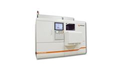
Manufactured by:3D-Micromac AG based inChemnitz, GERMANY
The microPRO™ RTP, a new laser annealing system designed to enable several key process steps in semiconductor, power device and MEMS manufacturing, combines a state-of-the-art laser optic module with 3D-Micromac’s modular semiconductor wafer manufacturing platform. It provides selective annealing with high repeatability and throughput in a versatile ...
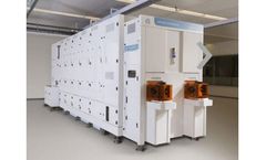
Manufactured by:Applied Materials, Inc. based inSanta Clara, CALIFORNIA (USA)
The Nokota system expands the Applied Materials suite of electrochemical deposition systems with a high-productivity wafer-level packaging tool that delivers best-in-class performance for the full range of plating steps used in diverse packaging schemes. These range from flip chip and wafer-level chip-scale packages to 2D and 3D fan-out, 2.5D interposerdesigns, and through-silicon via. Systems ...