


Semilab Semiconductor Physics Laboratory Co. Ltd.
- Home
- Companies
- Semilab Semiconductor Physics ...
- Products
- Semilab - Model AFM-2000 - Atomic Force ...
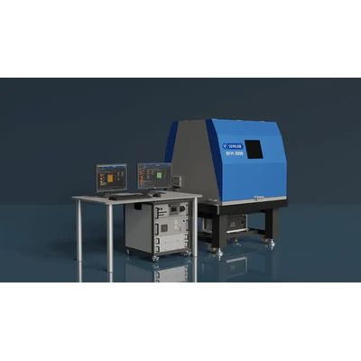
Semilab - Model AFM-2000 -Atomic Force Microscopy
The AFM-2000 is Semilab’s high-end atomic force microscope, delivering high-resolution, sub-atomic precision measurements for both academic research and semiconductor industry applications. Ideal for surface roughness and critical dimension control, it offers a large sample stage movement range of 200 × 250 mm with full automation capability—making it ideal for both R&D and industrial quality control.
Most popular related searches
atomic force microscopy
atomic microscopy
process monitoring
material science
microscopy
inline process control
process control monitoring
industrial metrology
metrology
automatic analysis
- R&D: Materials science, semiconductor device research, advanced metrology
- Industrial: Surface roughness measurement, critical dimension control, nanometrology, inline process monitoring
- Process control: Wafer manufacturing, structural feature analysis, automated measurement
- Proven track record of Semilab AFM product family: Cited in multiple scientific publications
- User-friendly operation for any trained operator
- Flexible workflow control via script or recipe-based operation
- High precision sample positioning with long-range XY stage (200 × 250 mm)
- Integrated optics for visual positioning & control during scanning
- High-resolution CCD camera
- Fully automated measurements with programmable positioning and report generation
- Multiple SPM modes including tapping, contact, conductive AFM, EFM, KPFM, MFM
- Sample size: 200 mm
- Sample thickness: <18 mm
- XY movement of sample: 200 x 250 mm
- Scanner: Planar scanner
- Scan area customization options:
- Scan range: 50x50 or 100x100 µmZ range 25 µm
- Z range: 5 or 10 or 25 µm
- Sample stage range: 200x250 mm
- Software: Measurement Control & Analysis Software