
- Home
- Companies
- Axetris AG
- Services
- MEMS Manufacturing Services
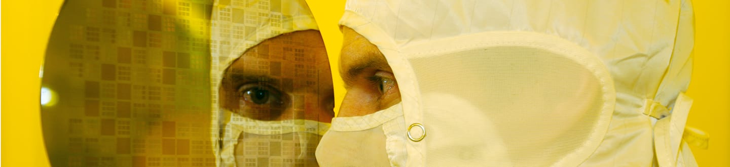
MEMS Manufacturing Services
We offer custom manufacturing solutions to OEM manufacturers ranging from concept to high volume manufacturing. Our foundry is equipped for 200mm and 150mm wafer sizes and includes the standard MEMS processes such as wet chemistry, lithography and thin film processing. Our high standard of quality control is ensured by a suite of metrological systems and the use of modern statistical methods which underpin all of our production processes which follows the guidelines of the TS 16949. As an ISO 9001:2008 certified company, we ensure the highest level of quality at a consistent level.
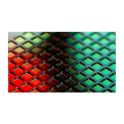
Photolithography
- Photolithography of 1 µm for up to 8" wafers
- Single or double sided alignment
- Thick resist processing (SU8, others)
Wet Chemistry
- Anisotropic Silicon etching
- Glass etching
- Metal etching
- Wet Cleaning Processes
Plasma Treatment / Surface Conditioning
- Metallization
- Sputtering up to 8" wafers
- Co-sputtering
Dielectric Coating Deposition
- Silicon oxides and nitrides by PECVD
- Oxides or nitrides by reactive sputtering
Reactive Ion Etching
- Fused Silica
- Silicon
- Silicon Nitride / Oxide
- Photoresist
Metrology and Characterization
- Interferometric and tactile surface measurements
- Film thickness measurement
- Resistivity & resistance
- Optical microscopy
- Automatic optical inspection
- Scanning electron microscopy (SEM)
Micro-optics:
- Refractive and diffractive for micro-optical elements
Thin Membranes:
- Thin dielectric membranes for optics, sensors and life science applications
CMOS Wafer Post Processing:
- CMOS post processing like back side openings, metallization, thin film deposition
Lift-Off Processes:
- Metallization in connection with lift off processes for electrode formation or solder pad definition. Materials include Au, Pt, AuSn, Cr, Ni, Ta, TiW, Cu, Al, other materials upon request
Dicing:
- Dicing of Silicon, glass & fused silica wafers
- Dicing of chips with fragile structures such as thin membranes and micro-optic structures